On this page I'll try to describe the theory behind a RAM upgrade I made for the 48k Spectrum back around 1988. "It can't be done," they said, and there isn't a better way to inspire to such a project, is there? ;-)
It seems you can't make a simple add-on that turns your 48k Spectrum into a 128k just using the expansion port. In order to get the screen paging you have to pull a leg of the ULA and turn the 16k screen RAM into two banks of 8k, replacing the upper half with some other area of RAM. A side effect of that should be that the RAM from 24k-32k works faster because it doesn't need to be shared between the CPU and the ULA anymore.
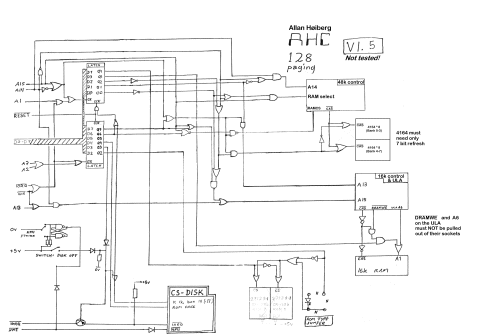
First, the diagram:

The diagram shown above is an optimized version of the first I made. Initially I used a lot of transistors and resistors, but as time went by I thought it all over and rationalized a lot in several steps. As it says on the diagram, this design hasn't been fully tested so I suggest looking at version 1.0 too in order to understand the logic a bit better (since there isn't so much re-use of each signal).
I made this sometime around 1988 so the details may be a bit unclear today. The construction was initially designed to work together with the CS-DISK floppy controller because that already had support for a second (EP)ROM.
If I recall correctly you can simply ignore the bits in the lower left corner from the NMI switch to the box marked "CS-DISK" altogether and nothing will be missing if you haven't got the CS-DISK.
The normal 32k RAM chips in a 48k Spectrum are said to be 64k chips that don't work in either the high or the low half. On the 48k PCB there are three holes somewhere between the ULA and the edge connector: GND, 5V and the middle hole that is really A15 if the RAM chips had been working as 64k - as it is, it is wired to either GND or 5V depending on the RAM chips used. The middle hole is the one I call RAM SELECT in this diagram.
The box marked "48k control" is the existing multiplexing circuits and address logic. The pins used are supposed to be disconnected from the PCB so that it is controlled by the new circuitry instead.
I have used two sets of 64k chips, soldered on top of each other with the CAS pins kept separate on the two sets. On the one prototype I have made using an even earlier version of the circuitry than v1.0, it turned out that some 64k chips require 8 bits for refresh which the Z80 doesn't deliver. I recall that some 64k required only 7 bits - these should be used unless you want to add some logic to simulate the 8'th bit during refresh.
The 16k control has never been tested, but I guess if you don't break any pins on the ULA you shouldn't be able to cause any damage to it by trying. A13, A15 and CAS must be pulled out of the socket and connected to the new circuitry instead, as must A1 and CAS on the 16k RAM chips.
The ROM type jumper is located somewhere near the CPU and the ROM, laid out as four holes with a diode and a piece of wire between some of them, depending on the type of ROM. If I recall correctly this controls the power to the pin that is used for programming power on EPROMs and some kind of chip select on ROMs, and an extra address bit which we use for selecting the right chip.
The plan is to use two EPROMs, mounted on top of each other, as with the RAM chips having CS as the only pin that separates them from each other.
Back to the Speccy Page. Last update 2001-11-04